Mass production of MEMS pins targeted with annual sales goal of W200 bil.
Point Engineering, a manufacturer of display and semiconductor parts, announced on May 24 that it would start a ‘pin foundry’ business for semiconductor testing.
Taking the same business structure as the semiconductor foundry process _ a consignment production method _ through Point Engineering’s new pin foundry business, high-end pins used for pre- and post-semiconductor process testing will be produced and supplied.
Point Engineering manufactures customized test pins upon customer requests as well as churning out MEMS pins for semiconductor wafer-level testing and socket pins for semiconductor post-process packaging testing.
“The size of the semiconductor test pin market is expected to exceed 1 trillion won ($790 million) this year alone, but the market has high entry barriers from technical limitations of high integration and miniaturization of sockets and probe cards,” a Point Engineering official said.
“However, we expect to secure an unrivaled position in the semiconductor test pin market by satisfying the four high requirements of high density, high frequency, high speed, and stability through our MEMS element technology, compared to the existing semiconductor test pin.”
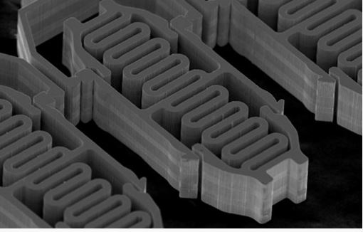
The company noted that the most distinguishing difference of its test pins is the replacement of pre-existing photoresist mold with an anodic aluminum oxide (AAO) mold to produce a pin in a completely new method.
Point Engineering said that there are three major advantages of the AAO mold. First, it is a high aspect ratio. The existing photoresist method can only support the pin thickness by 20~30um, whereas a single AAO mold can support up to 100~110um. Through this feature of AAO, a width of 5um by 100um thickness mold can be formed.
Secondly, it is the availability of fine patterning. Fine pattern gaps, as small as 4um, can be stably implemented to produce complex features of test pins. Precise technology can increase the number of beam strands of the pin body to increase the volume and surface area of the pin.
Furthermore, pins can be customized through Point Engineering’s own plating technology accordingly to the specifications desired by customers, such as current carrying capacity and pin force.
The final advantage is precision, according to Point Engineering. The upper and lower dimensional tolerances of a product made from the AAO mold, which consists of nano-sized pores, are only 0.5um.
“We are trying to actively communicate with customers through active online sales activities and our website, unlike the existing companies that used closed sales methods, which restrict technology opening,” Point Engineering CEO Ahn Bum-mo.
“Although we are still in the early stages of the business, we are aggressively marketing to successfully enter and settle the market, and we will do our best to achieve initial sales of 50 billion won per year, which is 5 percent of the market size, to 200 billion won, which is 20 percent in the future.”